Podcast Notes | Foreign Expert Opens Up Huawei's Kirin 9030: Without EUV Lithography Machines, How Far Has China's Chip Industry Really Come?
Podcast Notes | Foreign Expert Opens Up Huawei's Kirin 9030: Without EUV Lithography Machines, How Far Has China's Chip Industry Really Come?


Guest: Dylan Patel, Founder of SemiAnalysis
Host: None (Independent Commentary Video)
Podcast Source: SemiAnalysis
Original Title: Did China just beat Intel?
Release Date: July 20, 2026
Disclosure: This video is an interpretation of the first public report from SemiAnalysis’s STEEL Teardown Lab, directly promoting its paid teardown products. SemiAnalysis has direct commercial competition with TechInsights, a legacy teardown giant currently undergoing private equity sale (SemiAnalysis revenue has surpassed TechInsights). The following content faithfully presents their technical analysis and does not reflect the editorial stance of this publication.
Key Takeaways
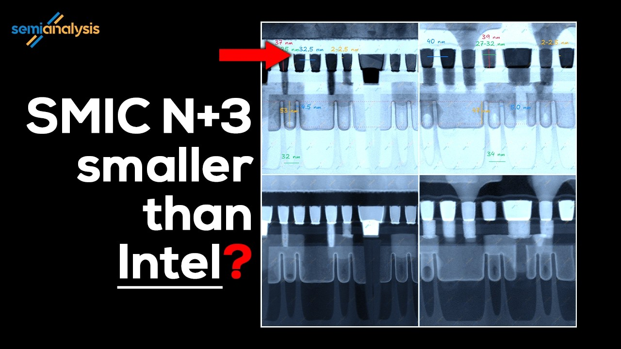
SemiAnalysis physically dissected Huawei’s latest flagship chip, the Kirin 9030, and measured the narrowest metal linewidth under an electron microscope. The result was surprising: SMIC’s third-generation 7nm process, N+3, achieved a minimum metal pitch of only 32.5nm—narrower than Intel’s newest 18A process used on Panther Lake, which measures 36nm. A Chinese foundry cut off from EUV lithography equipment has achieved higher wiring density than Intel’s leading EUV node.
Yet SemiAnalysis itself warns in the report that this number was selectively highlighted. While N+3 matches TSMC’s N6 in transistor density, it comes at the cost of quadruple patterning, more masks, higher costs, lower yield, and degraded performance and power efficiency—Kirin 9030 likely performs at the level of a three-year-old Android flagship. In short, Chinese chips remain years behind, but lagging does not mean being blocked. Export controls have not stopped China—they’ve simply changed the problem. The final line in the video is most worth pondering: China doesn’t need to catch up to TSMC; it only needs to become good enough to no longer need TSMC at all.
Highlight Quotes Summary
About the startling headline figure
About achieving EUV-level density without EUV
About matching density but falling behind in performance
About why people still fear China
About the real turning point
How Big Is the Gap for China Without EUV?
Today, the semiconductor manufacturing world is split into two camps: those with EUV lithography, and those without. Losing access to EUV is a clear disadvantage for China—but how significant is this manufacturing gap really?
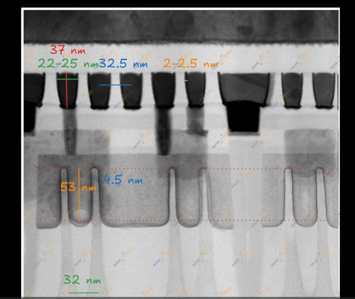
This is the HiSilicon Kirin 9030, the latest flagship SoC in Huawei’s smartphones. Weeks ago, SemiAnalysis cut it open and examined it under an electron microscope, measuring the finest internal conductive traces—the metal pitch. The result was unexpected.
The smallest metal pitch inside the Kirin 9030 is only 32.5nm, narrower than Panther Lake’s 36nm, despite the latter using Intel’s brand-new 18A node. A Chinese fab deprived of the most advanced tools and lacking EUV has achieved wiring density approximately 10% tighter than Intel’s leading EUV node.
This video aims to clarify three things: how SMIC achieved this without EUV; why finer lines don’t necessarily mean better performance; and why, even years behind, China has already become a meaningful player in semiconductor fabrication.
STEEL Teardown Lab: Where Do These Numbers Come From?
First, let’s discuss where these numbers and measurements come from—because the process itself is quite remarkable.
SemiAnalysis has built a teardown lab called STEEL—SemiAnalysis Teardown Engineering and Evaluation Lab. As the name implies, it involves physically disassembling the world’s most advanced chips and reverse-engineering how they’re manufactured. For roughly two decades, only one company could scale this operation—now there are more.
So everything you see next—cross-sections, linewidths, transistor counts—comes directly from STEEL.
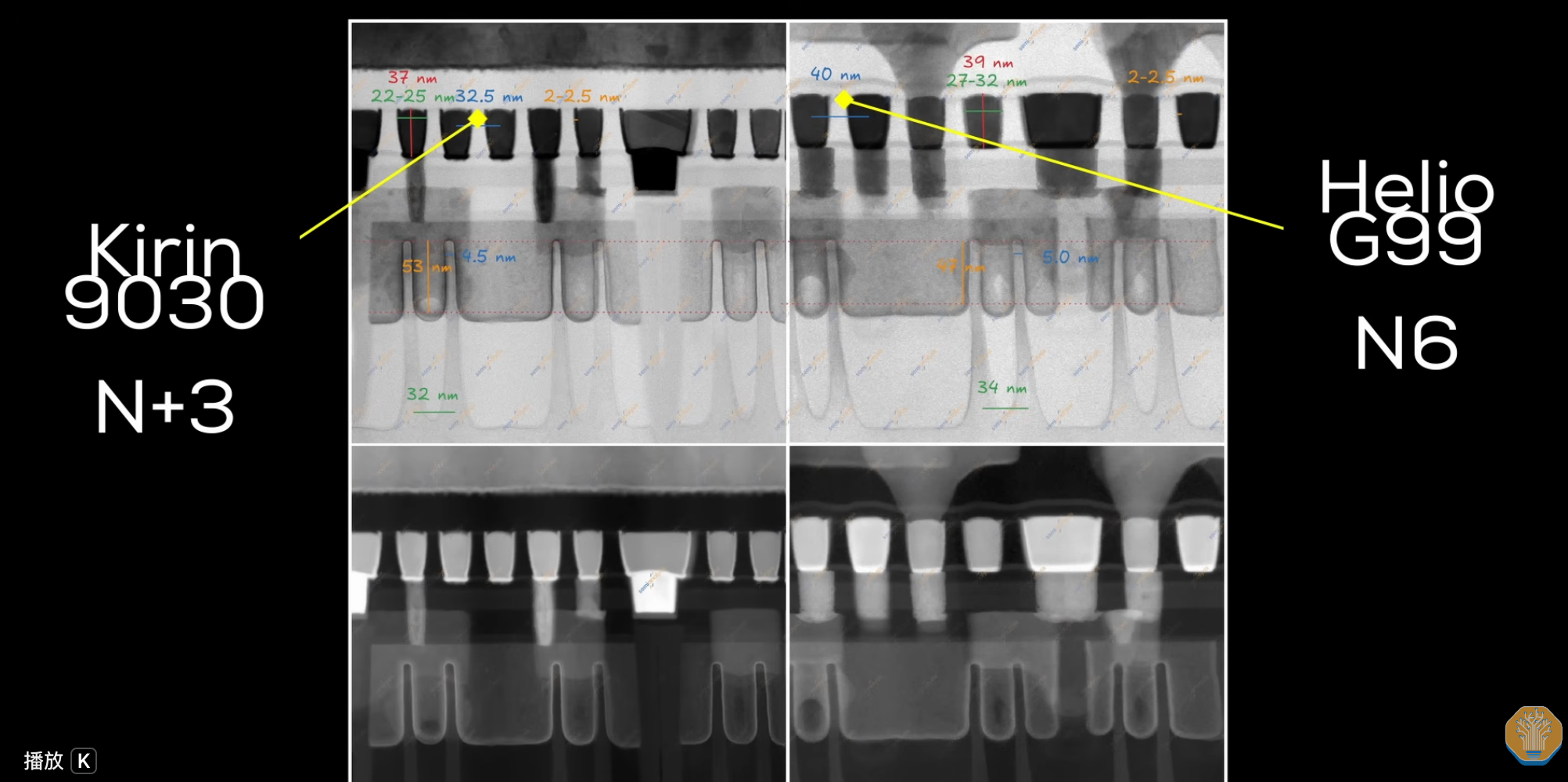
Lying on the “operating table” is the Kirin 9030, Huawei’s flagship SoC, based on SMIC’s third-generation 7nm process, internally codenamed N+3—the most advanced process currently available in China.
But a single number alone means little without context. So STEEL also dismantled another chip: MediaTek Helio G99, a budget smartphone SoC built on TSMC’s N6 process. The reason is simple: TSMC’s N6 and SMIC’s 7nm N+3 are roughly in the same category—same generation nodes. One made with Western state-of-the-art equipment; the other developed in China under export controls. Placing both under the same microscope allows us to hopefully tell a complete story.
N+3 vs N6: Density Has Indeed Been Matched
Don’t rush to compare with Intel’s 18A yet—first, let’s look at N+3 versus N6. Did SMIC’s N+3 achieve finer metal pitch than N6? The short answer: yes.
The measured minimum metal pitch in the Kirin 9030 is 32.5nm, while the Helio G99 based on N6 has a minimum pitch of 40nm—a substantial difference.
But “finer lines” refer to density—how many logic gates fit per square millimeter—not necessarily overall chip or node quality. Minimum metal pitch is just one part of the equation; it doesn’t indicate how fast the logic switches or how much power it consumes.
Looking purely at density, SMIC has indeed matched. N+3 achieves about 113 million transistors per square millimeter, compared to TSMC’s N6 at around 108 million. So yes—SMIC’s latest DUV node has surpassed an EUV node in density.
How to Achieve EUV-Level Density Without EUV: Multi-Patterning and DTCO
So how did SMIC achieve EUV-level density without EUV? There are two approaches—each with its own trade-offs.
The first is multi-patterning. EUV enables one shot to produce a relatively fine pattern. Without EUV, creativity becomes essential. The method involves first creating a coarse pattern, depositing a thin spacer along its edges, then etching. The spacers themselves act as a new, finer mask. It’s like drawing a line and tracing its two edges to generate two thinner lines—then repeating the process. One round is self-aligned double patterning (SADP); two rounds are self-aligned quadruple patterning (SAQP). SMIC’s finest layer requires the SAQP version.
Each additional step adds another mask, another alignment requirement, another chance for error—increasing cost and reducing yield. “You know I don’t like low yield.”
The second approach is DTCO—Design-Technology Co-Optimization. Instead of treating chip design and fabrication as separate problems, DTCO integrates them into a unified optimization framework. Practically, this means shrinking the cell layout itself: fewer fins per transistor, placing gate contacts directly above the active region instead of offset to the side, or reducing isolation spacing between adjacent cells.
Each DTCO technique recovers a bit of area—but each also makes transistors more fragile and harder to model. So SMIC has indeed matched TSMC’s EUV node in density, but only by brute-forcing DUV through more masks, more steps, and higher failure rates. This isn’t parity—it’s a tactical compromise.
Density Matched, Performance and Power Lag Behind
Density looks impressive, but this is precisely where it starts to unravel. Because area is the easiest dimension to optimize—power and performance are far harder.
Since Dennard scaling collapsed in the mid-2000s, Robert Dennard’s old rule—that smaller transistors are faster and more energy-efficient—no longer holds. Free scaling is over. After DTCO, speed and efficiency must be optimized separately—fish and bear paw cannot be had together.
This is exactly what we see on SMIC’s N+3 node. The Kirin 9030 Pro is a densely packed chip, but its performance is roughly equivalent to a three-year-old Android flagship. When compared to today’s top-tier offerings from Apple, Qualcomm, MediaTek, and Samsung, it’s in a different league entirely. The efficiency gap is wider than the speed gap.
A prime example is Apple’s tiny efficiency cores—those truly minuscule ones. Apple’s E-cores outperform Huawei’s large prime cores in integer performance, consuming only about 1W—Huawei’s prime core burns 4.5W. Per-clock performance-wise, Huawei’s prime core lands near the Arm Cortex-X2 level—2021-era design. To be fair, that’s decent engineering. But Apple’s M1 from 2020 delivered about 35% higher performance per clock at similar power. And the current leaders are ahead of both by several generations.
Thus, N+3 has a slight edge in density over TSMC’s N6—but N6 is already years old. Apple and Qualcomm are already building on N4 and N3, with denser transistors and far superior voltage-frequency curves. Chips based on N2 will arrive later this year. They have more transistors, each switching faster at lower power. SMIC has effectively optimized the wrong dimension. Lines got finer, density increased—but the underlying physics of the node hasn’t kept pace.
Comparing to Intel 18A: The Headline Is Real, But the Metric Isn’t Decisive
When comparing N+3 to Intel’s latest 18A, the contrast is even starker. On paper, 18A can achieve a 32nm M0 metal pitch—matching N+3. But on Panther Lake, Intel uses high-performance cells extensively, widening the M0 pitch to 36nm.
According to design goals, a looser M0 pitch offers cost and yield advantages by reducing complexity. But this assumes freedom to decide where and how to shrink—which means the headline “tighter than Intel” may be true, but doesn’t reflect competitiveness. The number is accurate—but the metric being measured doesn’t determine who wins.
In terms of transistor density, 18A clearly outpaces N+3—even with slightly looser metal pitch. Because, like chips aren’t just about density, and density isn’t just about M0 pitch. Backside power delivery allows for smaller front-side metal pitches, since power connections enter from the back of the die.
Why People Still Fear China: Lagging Doesn’t Mean Stalled
So why are people still afraid of China? Because lagging by years is not the same as being stalled.
SMIC still has room to grow on DUV. Finer lower-metal layers—for example, M0 is just the first layer; there are many more below. Shorter cells, tighter gate pitches. Paper specs suggest future N+4 could approach TSMC’s N5-level density, while N+5 with backside power delivery could reach Intel’s 18A-level density. But again—only in density. Power and performance remain uncompetitive.
The key point is cumulative difficulty. Each individual optimization seems reasonable on its own, but without EUV to stack them all, every new node becomes slower, more expensive, and less forgiving than the last. You can keep climbing the wall—but the wall gets steeper with every step.
Export controls didn’t stop China—they just changed the problem China must solve.
Moreover, knowledge is diffusing. SMIC is required to license N+2 and N+3 to other domestic foundries. If these process experiences flow into AI accelerators, the chokepoint won’t be a single fab subject to sanctions—it’ll be an entire ecosystem.
The Real Turning Point: Good Enough to No Longer Need TSMC
Let’s recap SMIC’s 7nm N+3 node: no EUV, no backside power delivery. Higher complexity, higher cost, tangible efficiency gaps. Looking at every critical metric at the cutting edge, China has not closed the gap with TSMC, Intel, or Samsung. The microscope reveals this clearly.
But “behind the frontier” is not the same as “irrelevant.” If domestic chips are good enough to power smartphones, inference engines, networking gear, or any security-sensitive application—then it’s a win. China doesn’t need to become TSMC to matter. It only needs to be good enough to never need TSMC again.
All content in this video comes directly from STEEL: die annotation, block-level analysis, direct electron microscopy cross-sections cutting through logic and memory. Much remains unexplored in this video: full process flows, material analysis, fin measurements, package teardowns. For deeper dives into SMIC’s latest node, check out SemiAnalysis’s teardown articles—links in the video description.
This is STEEL’s first public report—more will follow. If you enjoy this kind of content, subscribe. “I’d love to hear your take on this one. Is being good enough to no longer need TSMC actually good enough? Let me know in the comments.”
Compiled & Translated: DeepTide TechFlow
Disclaimer: Contains third-party opinions, does not constitute financial advice
Gyeonggi Province in South Korea abruptly halts stablecoin integration project, originally scheduled for completion by February 2027 or postponed
17 mins ago
Analyst: Lazarus Group has stolen a total of $11.87 billion, accounting for 45% of North Korea's GDP
26 mins agoMadagascar Ministry of Justice: 148 Crypto Investment Fraud Suspects Have Been Extradited to China Since September
1 hour agoHSBC will establish a global AI Institute in Hong Kong, initially focusing on blockchain technology
1 hour agoBinance updates its reserve proof address list, and future withdrawals will be processed from new wallets
2 hours agoLosses up by approximately 745% month-on-month, with 56 major attacks reported in the crypto industry in October
4 hours agoBinance plans to resume Phase 1 withdrawal services from 14:00 to 17:00 today
4 hours ago